Scintillator and SiPM based Radiation Detector for a High Altitude Balloon
Back to IndexTable of Contents
- Introduction
- SiPM Electronics
- SiPM Testing
- Other Electronics
- Launch #1
- Evaluation and Results #1
- Post-Launch Development
- Project Repositories
Introduction
Every year, my former school would participate in BalloonSat, where you would build a project which would then be sent up on a High Altitude Balloon (HAB), along with a number of projects from other schools. For the last few years, each entry had been somehow related to measuring radiation levels at altitude - first attempting to use a homebuilt ionisation chamber, then a Geiger-Muller tube. We wanted to get some kind of directional information, and try something a bit different, so we obtained a piece of plastic scintillator (Saint-Gobain BC408) which would emit light when struck by ionising radiation or high energy particles. The plan then was to use a small camera to detect the light, based on a YouTube video that now no longer seems to exist. Despite numerous image processing attempts, we were never able to detect any difference between a control and the school's radioactive sources, even using a DSLR with a reasonably large (albeit CMOS) sensor, and a 60s exposure. In actual fact, a camera on its own may have been able to detect sufficiently high energy cosmic rays, regardless of the scintillator. At the time, however, we decided to launch an entirely different project (attempting to use the signal strengths of several FM radio stations to perform triangulation), which is the topic for another article. We did consider at the time trying to obtain a more sensitive light detector, however, we decided we didn't have the time (at this point we had about a month before the launch), or the funds to do so.
A few years later, another opportunity to launch a project on a HAB came up, provided by Chris Hilcox, with fewer restrictions on weight and power, given as a prize to my former school's CanSat team for winning the UK final. I did this project with the leader of this team, William Eustace (wje.io). At first, we experimented with a photodiode based detector based on an Elektor design, which worked reasonably but simply wasn't very sensitive - we were unable to get the noise floor as low as in the article - and had a very limited area meaning the count rate was always fairly low. In addition, high energy cosmic rays would likely lose little energy to the sensor and therefore not produce that great a difference to lower energy particles. We therefore decided that it would be interesting to try again and use the scintillator. Our first test was trying to use a blue enhanced photodiode (the scintillator's emission peaks around 420nm) and the same amplifier used when using the photodiode to directly detect radiation, however no difference was observed compared to the photodiode on its own. In retrospect it may have been worth experimenting further with this design, however, we didn't want to waste too much time. While trying to get hold of a more sensitive detector, we tried a few 'moonshot' ideas, one of which was reverse biasing LEDs with 30-60V (depending on the device) to create a crude avalanche photodiode. Although avalanche breakdown did occur, and the number of pulses was related to light level - in fact this actually produced a reasonable detector - even with coincidence detection it didn't seem sensitive enough to detect pulses of light from the scintillator. Again, this probably warrants further investigation, perhaps using a large array of SMD LEDs, and experimenting with more types of LED and greater bias voltages (the setup used could only produce up to 60V, not enough for many LEDs). This, if it worked, would create a very low cost detector.
Some research suggested that the ideal device for our application was a Silicon Photomultiplier (SiPM), which is a solid state detector capable of detecting very small amounts of light. It works using a large number of avalanche photodiodes in parallel, and operating in "Geiger mode", so when a number of photons hit the SiPM near simultaneously, a pulse is produced with the amplitude proportional to the number of simultaneous photons. These have been successfully used with plastic scintillators in previous projects. Unfortunately, SiPMs are very expensive - on the order of ~£70 each, and ideally we wanted more than one so we could try and determine the direction of incident radiation, and perform coincidence detection to reduce the number of false counts. In fact, the best option appeared to be a ready made 4x4 array, which would have cost in excess of £400, beyond our budget particularly considering the additional cost of the readout electronics. Fortunately, Advansid were willing to provide a SiPM array free of charge (ASD-NUV3S-P-4x4TD), the one caveat being it had one defective channel (this was not a particularly major problem, 15 working channels are more than enough for our application).
SiPM Electronics
SiPM Electronics Overview
Now that we had found a suitable sensor, it was time to build the readout electronics. I was tasked with designing the electronics that interfaced with the sensor itself, and William worked on the other parts of the electronics - radio, GPS, SD, etc. Typical SiPM readout electronics consist of an amplifier, to convert the small output pulse into an easier to measure larger pulse, followed by some system to measure the amplitude of the pulse. We actually decided to take a slightly different approach, in order to reduce the size, power consumption and cost, for the latter part of the system. Instead of measuring the amplitude of the pulse on all 16 channels, which would require either 16 fast peak detectors or 16 fast ADC channels, we decided to measure the width of the pulse. This can be done fairly simply, using a comparator and a fixed threshold to convert it into a digital signal, and then use an FPGA to measure the total pulse width on each channel using 16 counters and a fast reference clock. The FPGA also handles event detection, requiring various criteria to be met before an event is recorded. This will be discussed in more detail later.
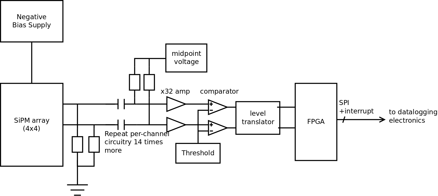
Above is a block diagram of the electronics, as described in outline above. The bias voltage, midpoint voltage and comparator threshold are all controlled by a precision DAC connected to the main processor, allowing precise and repeatable adjustment without large multi-turn potentiometers. The level translator is required as the analog electronics run off 5V, whereas the FPGA requires a maximum of 3.3V.
Analog Signal Conditioning
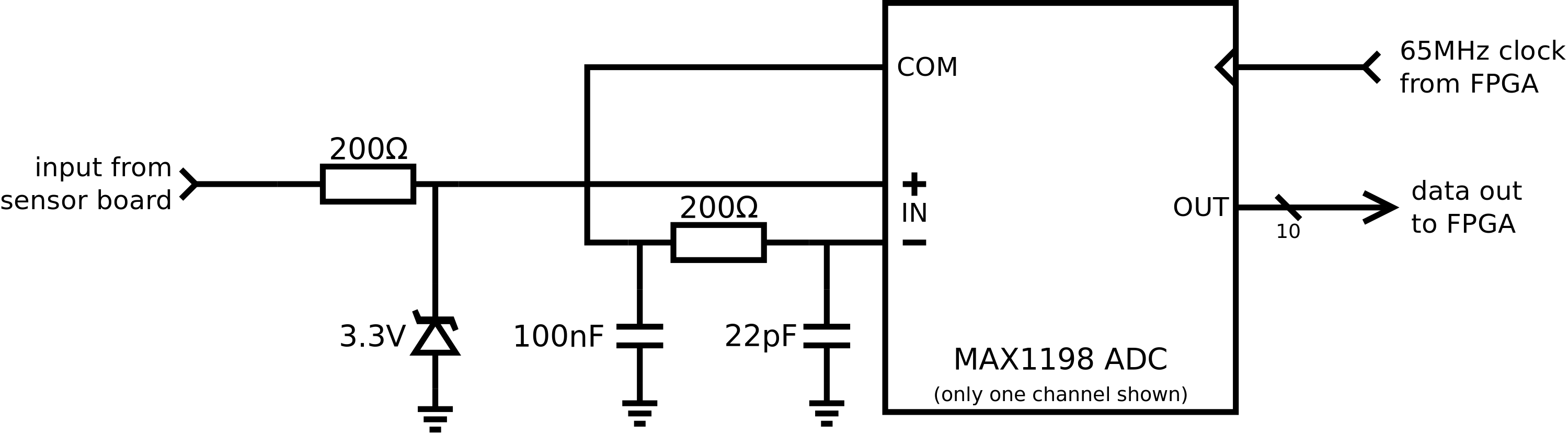
Here is the signal path for a single channel in more detail, showing the circuitry around the SiPM and the x32 amplifier circuit.
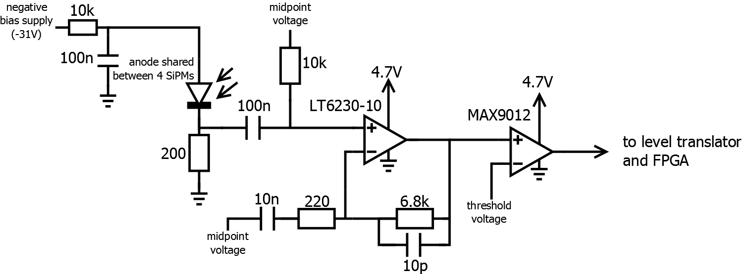
The 200Ω load resistor converts the current pulse from the SiPM into a voltage pulse, which can then be amplified. This pulse is AC coupled into the amplifier through a 100nF capacitor, which avoids the need for a negative supply for the amplifier, and also subtracts any DC dark current. An alternative would be to have a DC coupled path and connect the load resistor to the midpoint supply rather than ground, however, this would have reduced the bias voltage by 2.5V. As the maximum bias voltage that could easily be generated (described later on in this document) is around 38V, this was deemed unacceptable at the time of design, as the exact necessary bias voltage was unknown.
The AC coupled voltage pulse is then centered about the midpoint voltage, and amplified. The 10nF capacitor in series with the 220Ω resistor from the inverting input to the 'virtual ground' (actually the midpoint voltage, as this is a single supply amplifier), ensures the DC gain of the amplifier is low, to avoid small DC offsets (e.g. due to the op-amp input current) being amplified and resulting in a large offset at the output. The 10pF capacitor ensures stability of the amplifier. The AC gain of the amplifier, at frequencies before roll-off due to the 10pF capacitor occurs, is about x32. The LT6230-10 op-amp was chosen as it has a high GBP (1.45GHz), and yet comes in a small package (SOT-23-5) and is not overly expensive.
The 4.7V supply voltage, is obtained using a low noise LDO connected to the 5V supply (LD3985M47R). This minimises the amount of noise coming from the power supply.
Bias Voltage Generation
Some care is needed to generate the negative voltage (-31.5V in this case) used to reverse bias the SiPM. The obvious way of doing this is with some kind of inverting switching regulator, which will create noise which must then be filtered out. Alternatively a stack of CR2032s could have been used (12V alkalines such as the 23A form factor are not reliable at low temperatures), however these would be too unstable without regulation; and regulation would add a fairly significant current draw, meaning they would have to be replaced a few times which would be tedious and get fairly expensive. As a result the combination of a switching regulator, op-amp for regulation, and significant filtering, was chosen.
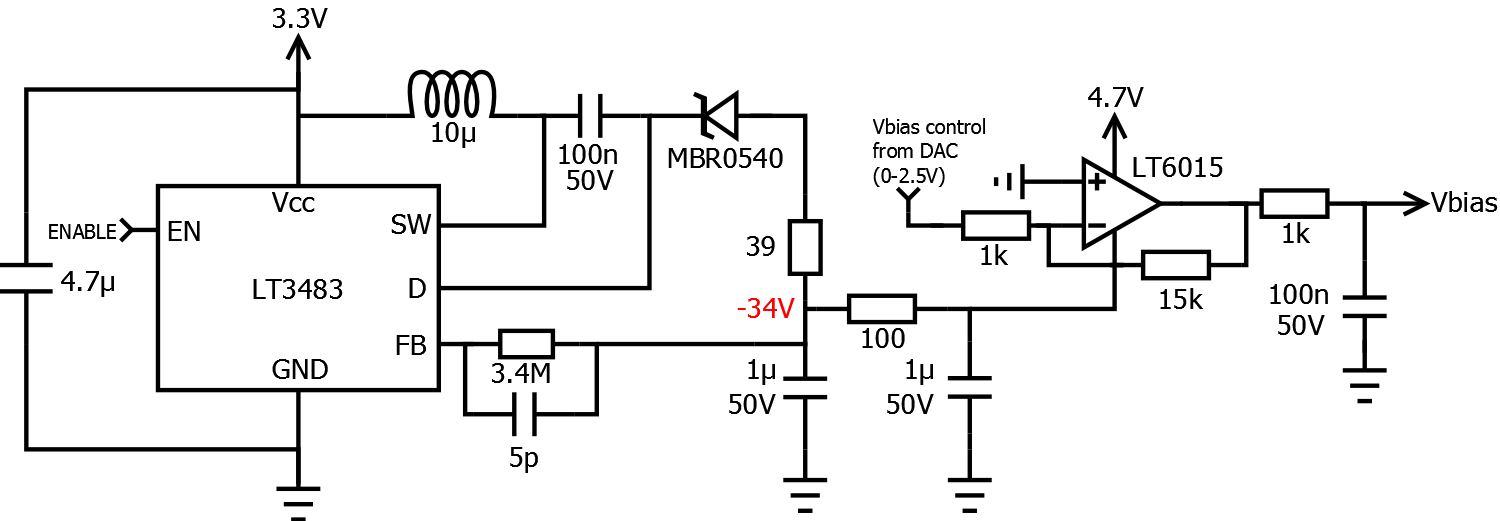
This is the bias generation circuit as used. The first part of the circuit is based on an example in the LT3483 datasheet, configured to generate -34V. This part was chosen as it is capable of generating fairly significant negative voltages without too many parts, and available in a reasonable package. There is some initial filtering in the form of a 100Ω resistor and a 1μF capacitor, followed by an op-amp used to set the exact bias voltage. This takes a control input from the DAC, in the range of 0 to 2.5V, and multiplies it by -15 to produce the bias voltage. As the DAC contains a stable internal reference, this control voltage and therefore the bias voltage will be well regulated. There is a further RC filter, the effect of which will be fairly insignificant on the bias voltage as the average current drawn by the SiPM will be low.
Digital Processing
All of the high speed digital processing is done inside an FPGA (Lattice MachXO2 series, LCMXO2-2000HC-4TG100). A simplified block diagram representing the logic implemented inside the FPGA is shown below. The VHDL source code is also available in the project's GitHub repository, which gives a precise description of the logic.
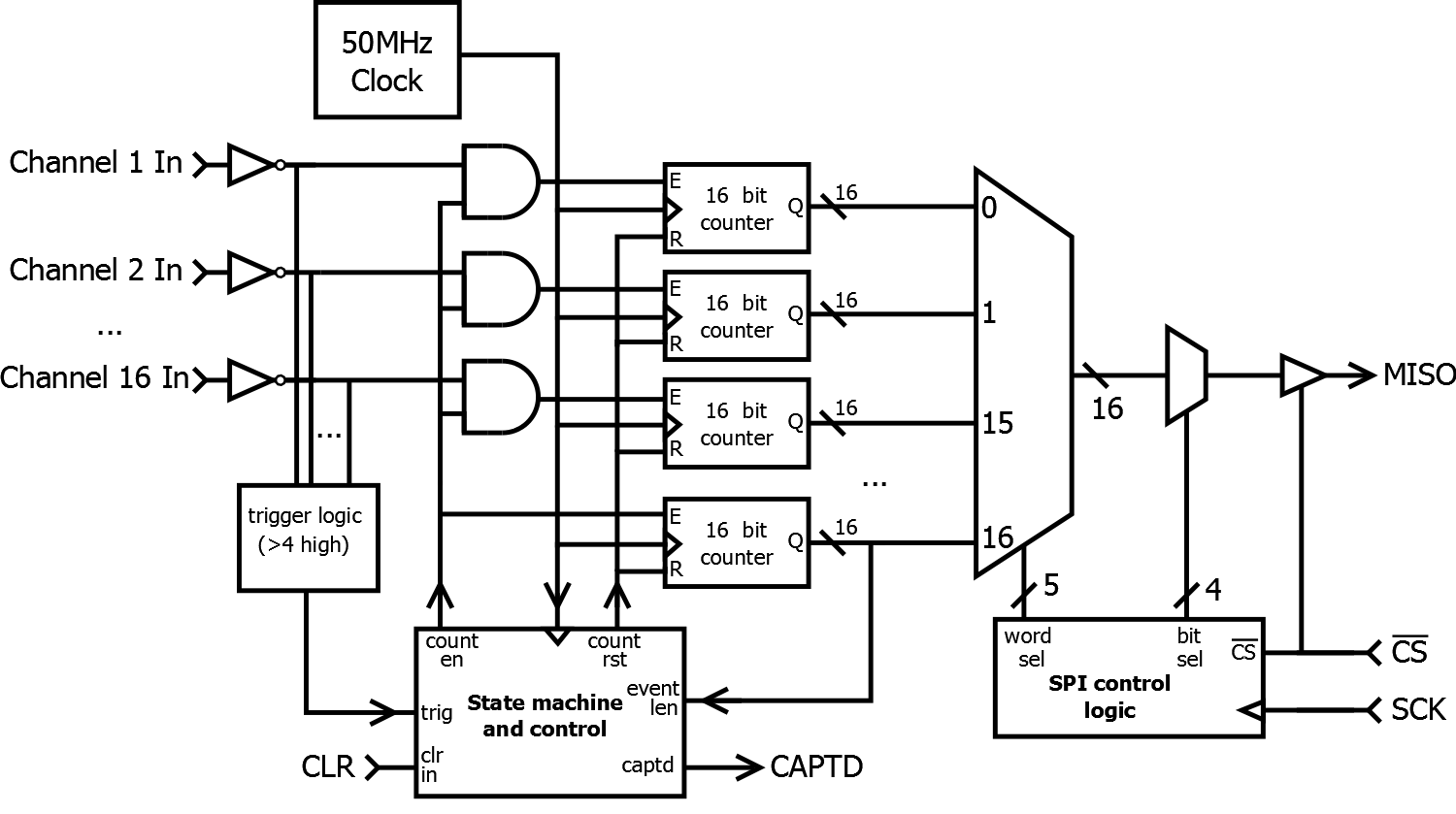
There are a number of different subsystems implemented inside the FPGA. First of all, there are 16 counters and a reference clock, used to measure the pulse width on each channel. Then, there is a coincidence detection system, which outputs a high if more than 4 channels are active (note that channel inputs are active low, and therefore inverted inside the FPGA). There is an additional counter used to measure the total length of the event, which is used by the control logic to reject events that are too short, (representing a small number of simultaneous photons and therefore most likely the dark noise of the SiPM), massively reducing the amount of data that needs to be handled by the microcontroller. The majority of the logic inside the "State machine and control" block can be represented using a state diagram.
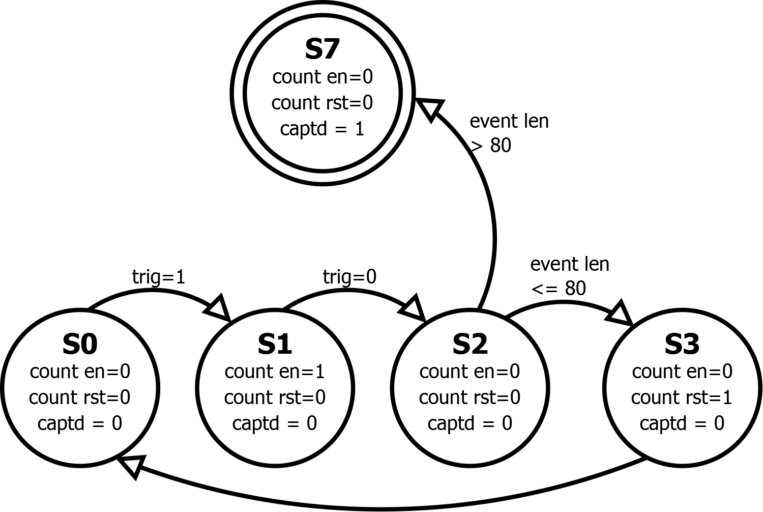
In addition to the transition rules shown in the state diagram, when the CLR input is high all counters are reset and the state is forced to S0. Once an event has been captured, the CAPTD output going high informs the microcontroller of this, so event data can then be read out of the FPGA using an SPI-like interface. State transitions occur on the falling edge of the system clock, whereas counters increment on the rising edge of the system clock.
The SPI interface is implemented using two multiplexers and some control logic, including a counter inside the control logic. This counter is incremented on every rising edge of the SCK input, and reset when CS is deasserted (high). The lower 4 bits of this counter go into the second multiplexer, which is used to select which bit of the current word is output onto the MISO line. The upper 5 bits are used to select which 16-bit word is being read, with a total of 17 words (the pulse width for each pixel and the total event length). As a result, there are a total of 272 bits to be read out for each event. In order to enable multiple devices to share the same SPI bus, MISO is set to tristate when CS is deasserted.
Electronics Construction
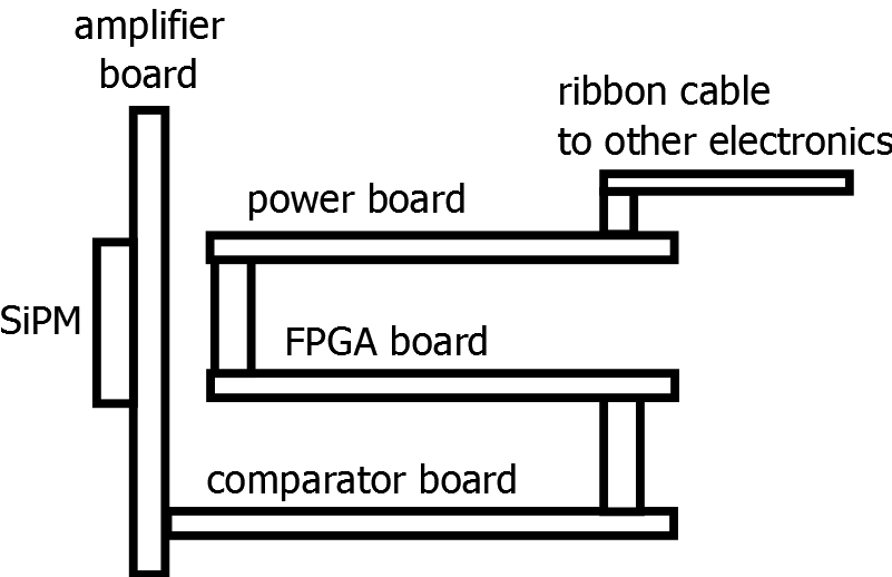
Above is a diagram showing how the circuit boards comprising the readout electronics are arranged. First, there is a vertical board which connects to the sensor itself, and contains the fast x30 amplifiers described in the Analog Signal Conditioning section. There is also the possibility for an analog temperature sensor to be fitted to this board and connected to an ADC input on the microcontroller, allowing sensor temperature to be measured (this was not fitted for the first launch).
This board then connects to the comparator board. This board contains the 16 fast comparator channels (arranged as 8 MAX9012s), as well as the SN74LVCH16T245 level translator to convert the 4.7V comparator outputs to 3.3V logic for the FPGA. This board also contains the bias voltage generation, the DAC7564 precision 12-bit DAC used to control the bias voltage, midpoint level and threshold voltage, and the low noise 4.7V voltage regulator.
Above the comparator board is the board containing the Lattice MachXO2 FPGA. This part was chosen as it has reasonable performance, enough macrocells for the application, and is highly integrated - with built-in bitstream flash and an internal oscillator. The internal oscillator and PLL are used to generate the 50MHz system clock, as high precision is not needed.
Finally, there is a board that contains 3.3V and 5V regulators. Battery input goes into this board, and the 3.3V and 5V rails are output on the ribbon cable for the datalogging electronics to use.
These photos show the electronics as assembled. Note that there are some additional modifications in addition to the errata list below. You will not need to make these - they were added after some tracks were broken during assembly and debugging. In addition, the 3.3V switching regulator on the power board was replaced with an LDO during debugging, however, the switching regulator should work fine (it was removed while troubleshooting a noise issue actually resulting from the 5V regulator oscillator; see below).
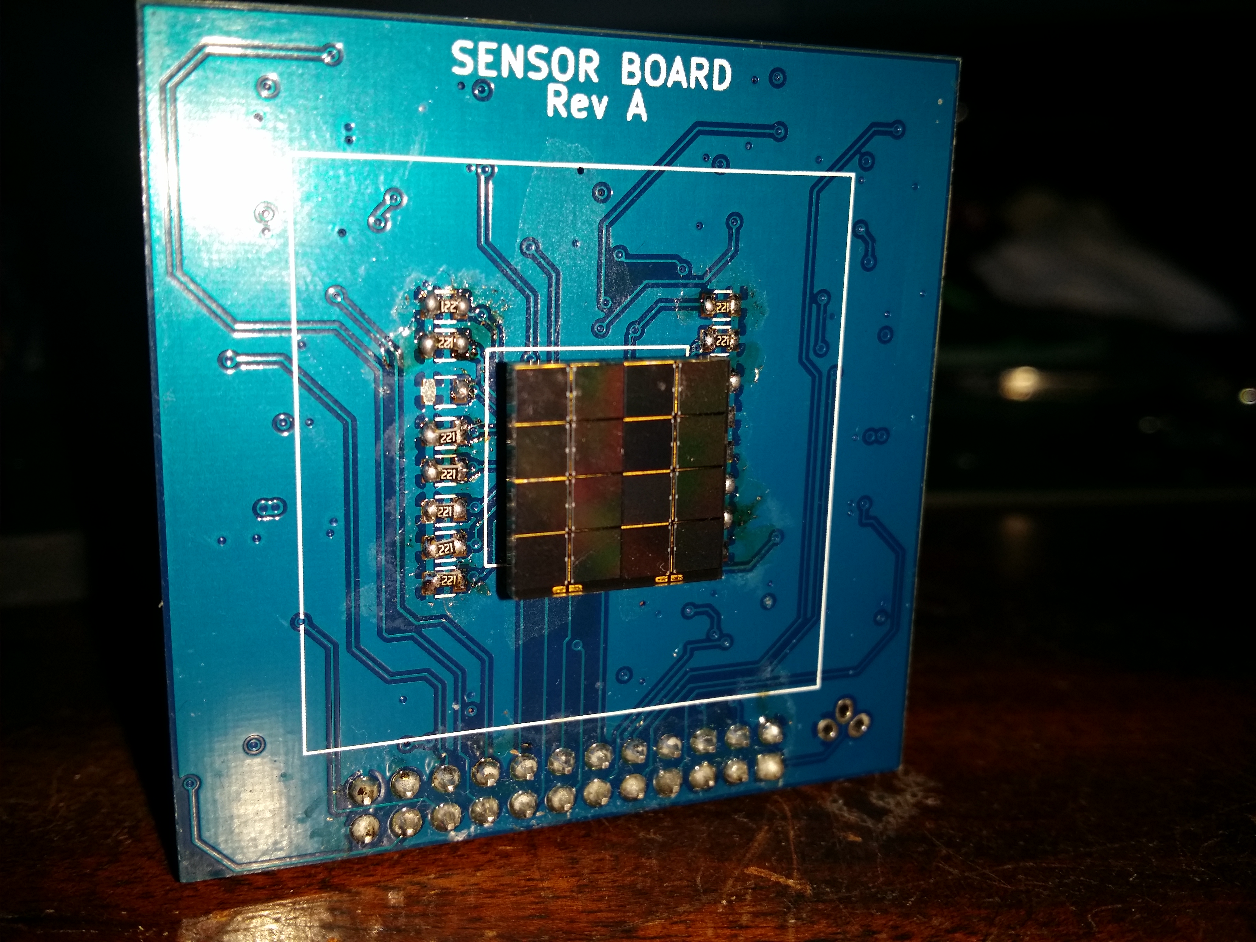 Amplifier Board Front showing SiPM
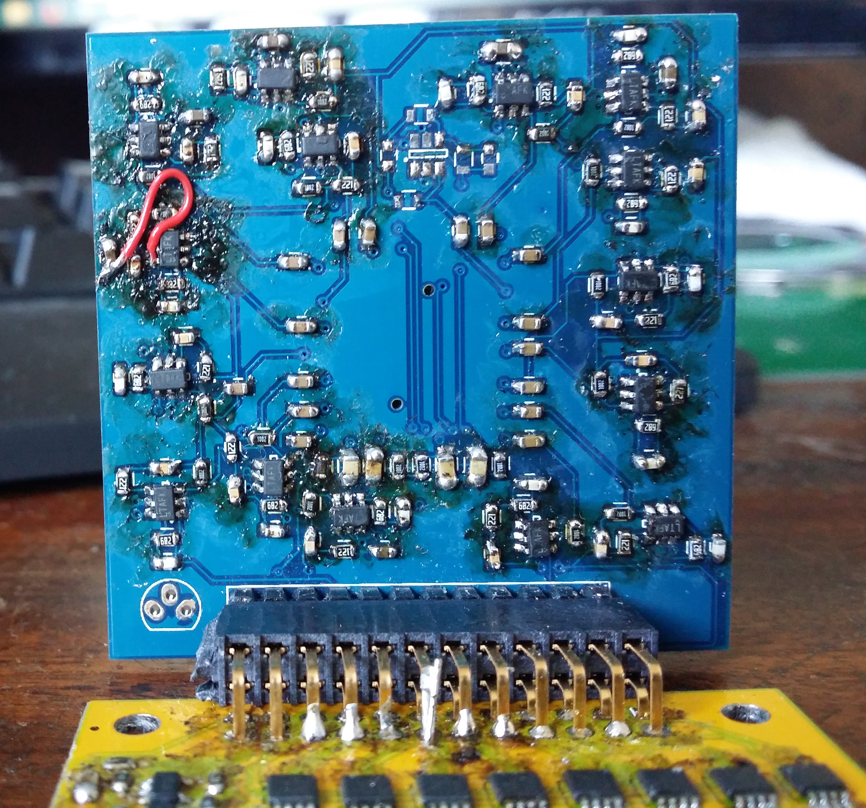 Amplifier Board Back
 Amplifier and Comparator Boards
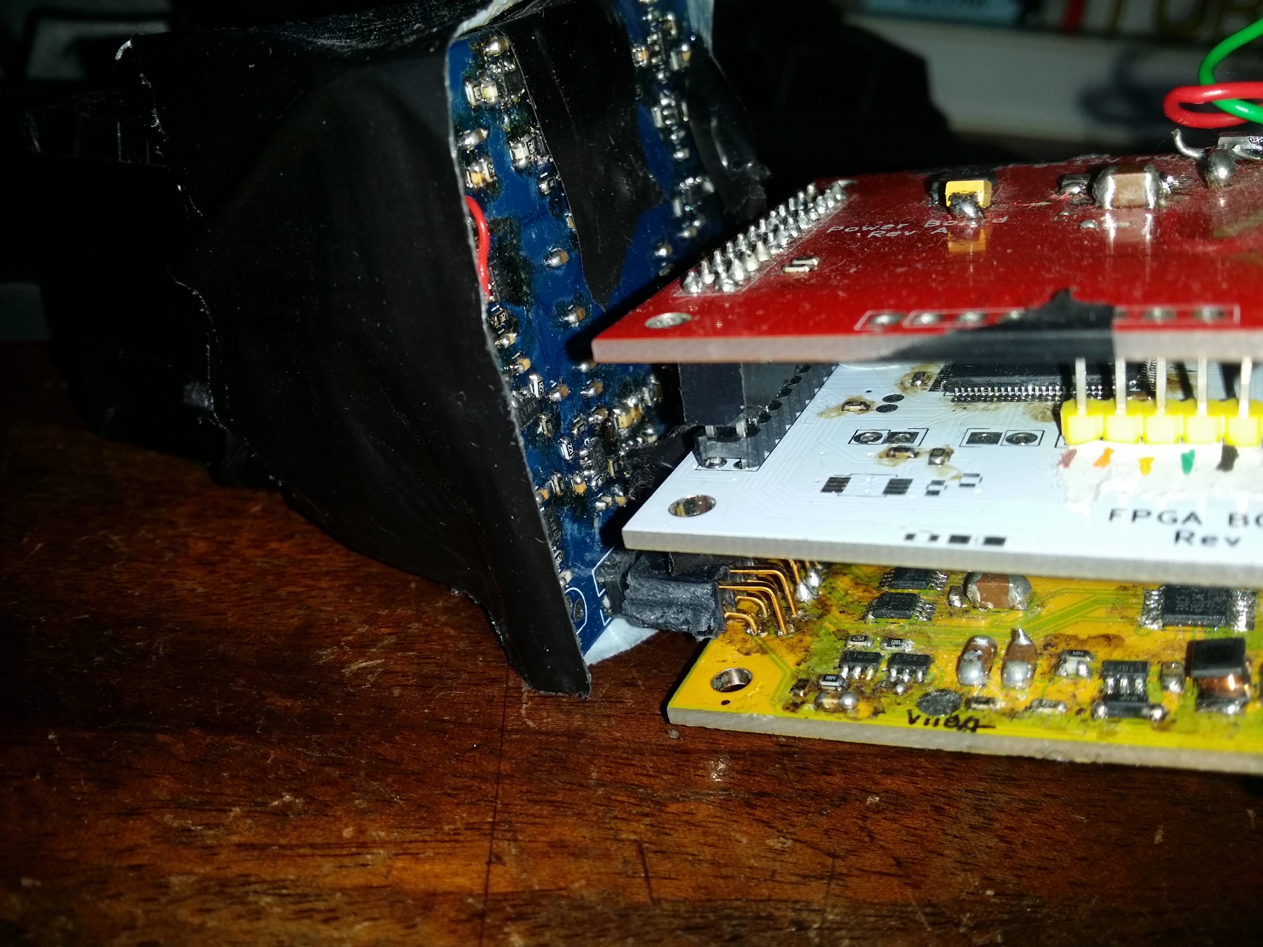 Electronics "Stack"
Design Files and Errata
Design files in KiCad format, and Gerbers for PCB manufacturing, are located in the 'hardware' folder of the project's GitHub repository. Gerber files are located in the 'out' folder for each board. Please note that there are some issues with these designs, which must be corrected if you assemble them.
- On the amplifier board, the capacitor between op-amp output and op-amp inverting input (e.g. C28, C30, etc.) is marked DNP. This should actually be fitted, I used a value of 10pF but this could be experimented with.
- The sensor pinout on the amplifier board is a mirror image of the correct pinout. This does not actually affect operation, fortunately, but means the channel numbers on the schematic are incorrect. This is corrected for inside the FPGA.
- On the comparator board, the bias voltage monitoring (Vb_mon output) does not function correctly. This is not particularly critical, however. For it to work, the best option would be to use an op-amp that had a common mode voltage range including and ideally going below 0V instead of the LT6003. The resistor values also need to be changed.
- Also on the comparator board, the DAC VrefL input was left unconnected whereas it should be connected to ground. As this pin is next to the ground pin, it is suggested you create a solder bridge between the two (pins 5 and 6).
- On the FPGA board, the monostable and LED were not populated, as any light inside the sensor enclosure will increase the noise floor of the sensor.
- The LK115D50 oscillates when a ceramic output capacitor is used on the power board; as there is a minimum ESR requirement. Either use a small (e.g. 0.22Ω) resistor in series with a ceramic capacitor; or a electrolytic/tantalum type capacitor.
- Programming the FPGA was sometimes found to be unreliable, using an FTDI MPSSE cable (C232HM-DDHSL-0). This was solved by adding a small capacitor (22pF) between TCK and ground, however, this may not be needed if you use an official Lattice programmer.
SiPM Testing
During and after the construction of the SiPM electronics, various tests were carried out to ensure that the SiPM was functioning correctly. Initial testing was carried out by connecting one or more (through an OR gate - note that the outputs are inverted - for coincidence counting) comparator outputs to a microcontroller interrupt pin, and counting the number of interrupts. This allowed the bias voltage and threshold level to be varied and the change in output pulse rate observed.
From this test, it was determined that a threshold level of around 25mV at a bias voltage of -31.5V gives a count rate similar to the dark count rate of the sensor - this is therefore likely to be close to the single-photon level. It was also noted that even a small amount of light entering the sensor enclosure caused a major increase to the count rate, and therefore that lightproofing was very important.
In order to get an idea of whether the system was working, without needing any radioactive sources, comparative tests were done with and without the scintillator present, the expectation being that adding the scintillator would increase counts above a certain threshold as it picks up background radiation. Although some difference was seen, I decided that I would like to see more data.
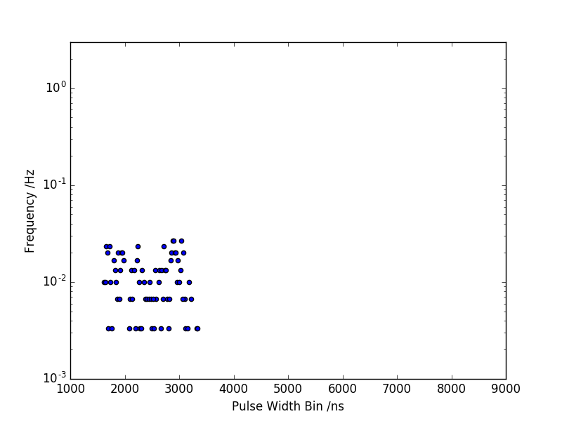
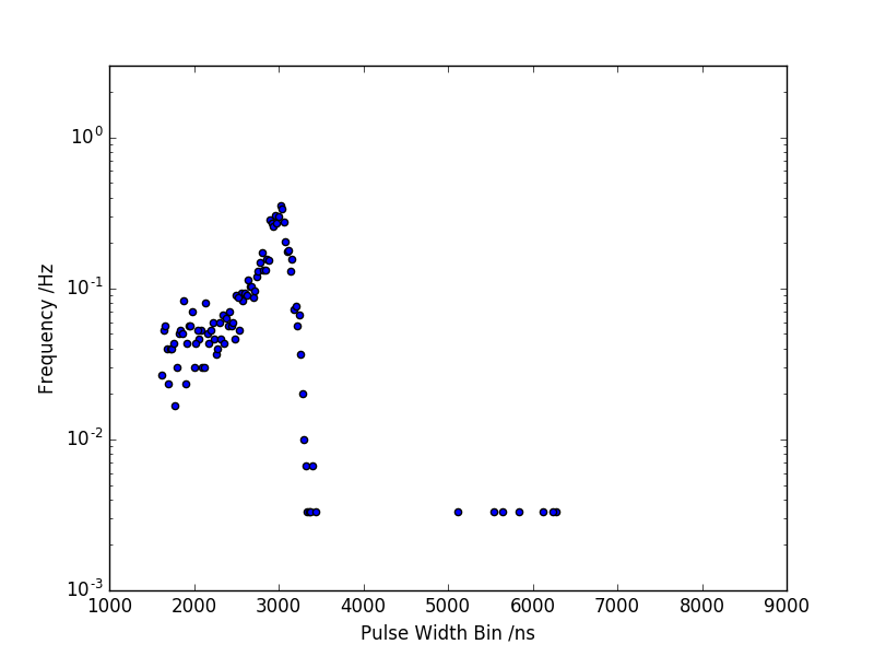
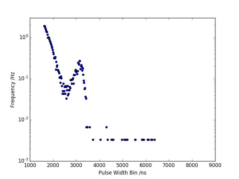
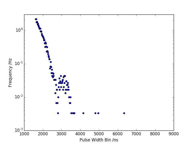
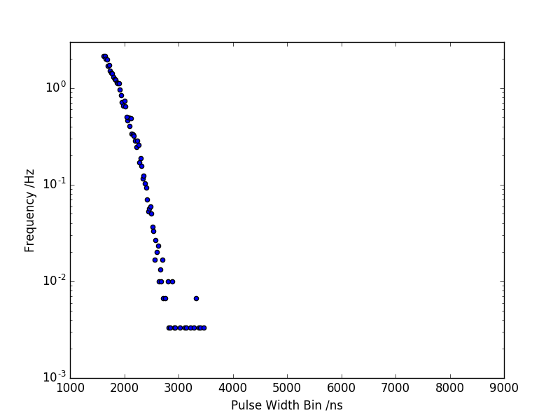
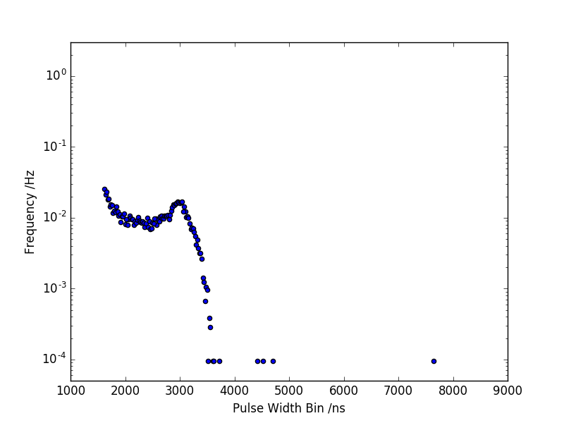
As a result the FPGA was programmed to create histograms of pulse widths, counting the number of pulses with in a certain width bin and storing this in block RAM, where it could then be read out. This gave a much more definitive answer that the SiPM and scintillator were in fact working.
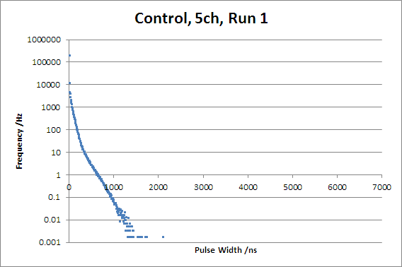
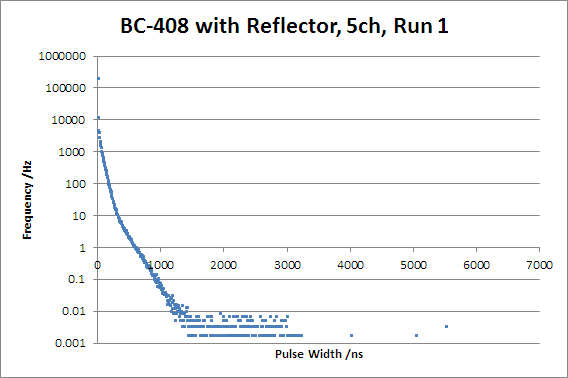
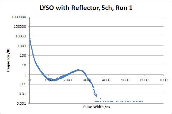
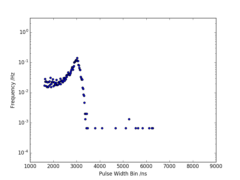
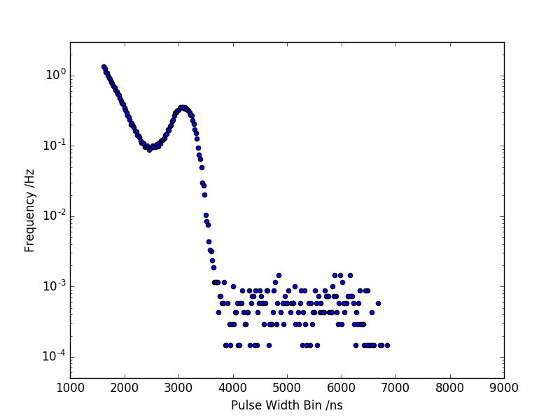
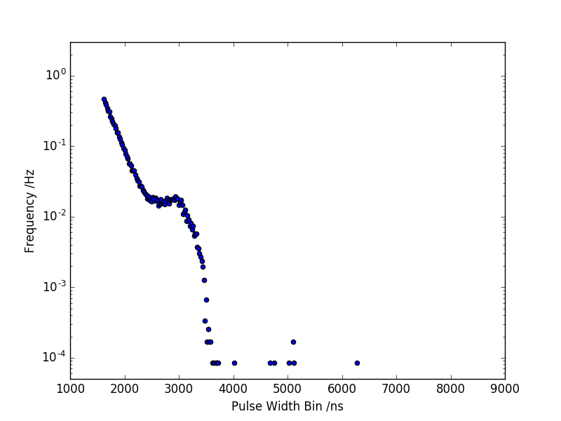
These are the graphs obtained from the setup, with count rate on the vertical axis (note the logarithmic scale), and width bin on the horizontal axis. In order to prevent any experimental bias, multiple controls and scintillator tests were carried out in various orders All the graphs are viewable on a seperate page. Some change in noise level (count rate of short pulses) can be observed, possibly due to change in the temperature of the sensor (unfortunately this was not recorded), or slight a change in the amount of light leakage. All tests were carried out with a measurement period of 10 minutes.
Overall, however, there is a significant difference between the scintillator tests and the controls, in particular looking at pulses exceeding 2000ns. In addition to the BC-408 scintillator previously mentioned, a LYSO scintillator was also obtained. As this is itself a slight beta and gamma emitter, there is a significantly higher background due to light resulting from its own radiation. It is also more sensitive than the BC-408 scintillator to external radiation.
Now that we were reasonably sure that the setup was working, it was time to test it with the school's radioactive sources. For safety reasons, only a very short test was performed, so unfortunately no data was recorded. However, a significant increase in the count rate above 2000ns was observed, giving us final confirmation that the setup was working
Other Electronics
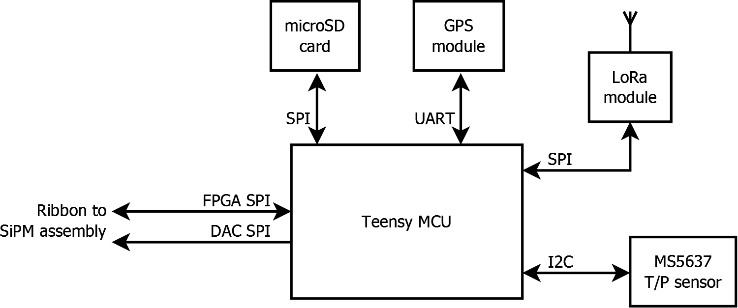
As well as the SiPM readout electronics, there were also some other electronics, to make some additional measurements, and record and transmit the measured data. A block diagram showing the arrangement of these electronics is above. As you can see from it, the entire system was controlled by a Teensy 3.1 microcontroller board. We also had a temperature and pressure sensor, primarily for determining altitude, and a GPS for determining position. Data was saved to an microSD card, and a subset of data was transmitted using the LoRa radio. LoRa was chosen as it offers a very high link budget (over 150dB in some configurations) with a low transmit power (10mW at 433MHz).
The microcontroller also set up the DAC, and interfaced with the FPGA using the SPI interface and other pins. Events were logged to the SD card whenever they occurred, and an additional log entry was made every 5 seconds containing limited count information as well as the other measured variables (temperature, pressure, position). In addition, also every 5 seconds, some data was sent over radio in case the payload was not successfully recovered. This included temperature, pressure, position, total count rate, and count rate over 2000ns (deemed to be the threshold over which events are considered 'significant'. Some information about system status was also sent, to make debugging at the time of launch easier. The PCB handling this is showed below.
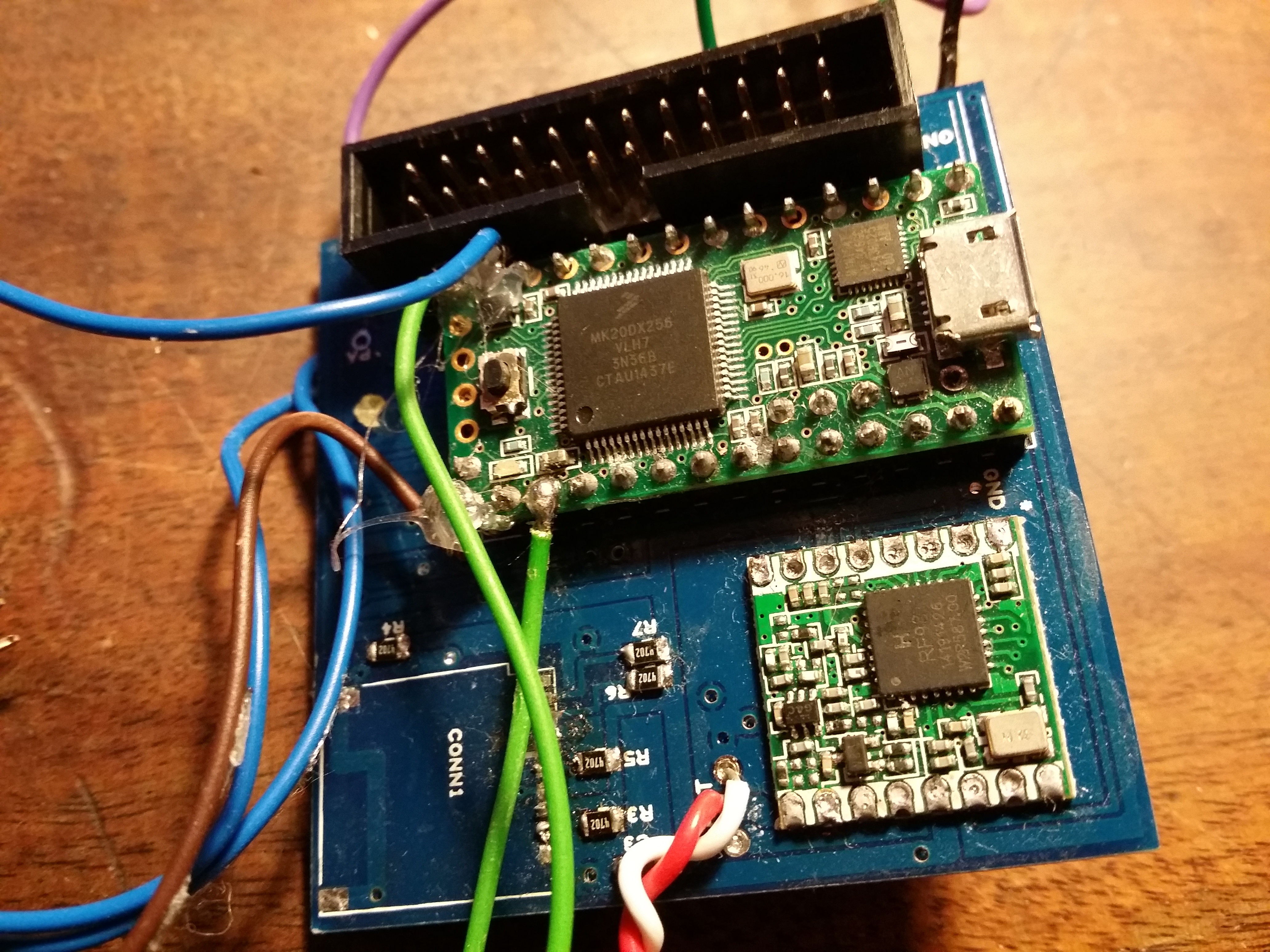 Datalogging Board
Due to unexpected issues during assembly, the microSD card holder could not be soldered to the board. Instead a socket was connected to the board using some wires soldered to the Teensy. The software programmed to the board is also available in the GitHub page. As well as the operation described above, it also performs a few other tasks. These include setting up the GPS for a mode supposed to work better at high altitudes, which was recommended by the manufacturer of the GPS module that we used.
We were also unable to get the radio to perform reliably at very low data rates. This is due to a combination of reasons. Primarily this is because the particular modules that we used use a regular crystal rather than a TCXO, so the frequency drift during transmission is too high. In addition, the modules have some functionality to compensate for this, called the "Low Data Rate Optimiser", however, we had not noticed this and therefore did not have this enabled.
Launch #1
The first launch was carried out towards the end of October 2015, launching from the Welsh border. This launch, as mentioned previously, was kindly provided by Chris Hilcox as a competition prize. We flew all of the electronics described above, which were for the most part functional. Unfortunately two additional sensor channels had failed (in addition to the 1 that was known defective), for reasons currently unknown. This was not deemed to be a major issue, as 13 channels still appeared to be functioning correctly. A 4GEE camera was also fitted to the payload, and the footage from this can be viewed on YouTube.
In order to increase our chances of successfully receiving telemetry from the balloon, we set up our receiver towards the top of a hill in the Peak District. A small mast was also made for the main Yagi antenna, in order to ensure it was clear of surrounding trees and objects. Radio communications were first received when the balloon was at an altitude of about 6km, and about 99km away across ground. Radio performance was in fact even better than expected, as even at this distance the RSSI was -96dBm and the SNR -1dB. Not only did these successfully prove that the radio was working well, the data also indicated that all electronics were working well - a valid GPS position was being reported, pressure data seemed feasible, and the number of significant events was increasing. A simple dipole antenna was also set up indoors, near the main antenna, as an additional receiver. This worked better than expected, first receiving packets when the balloon was about 90km away (although the SNR was considerably worse and packet loss was higher than the Yagi.)
The balloon reached a peak altitude of 27.5km. Unfortunately, it was noticed that, on the way down, the count rate was high than expected, and more counts were below 2000ns than expected. This already suggested a possible failure in the lightproofing. The payload was recovered successfully, and kept turned on during some of the journey back for some final experimentation. The device was monitored over radio, and we discovered an increase in count rate whenever we went past a street light (it was now dark). This confirmed that the lightproofing had partially failed.
Evaluation and Results #1
Following recovery, the microSD card was removed from the payload and the data was read out successfully. This data was then analysed, primarily using Python and matplotlib to plot various graphs. In order to get a better idea of what happened, pulse width distributions (similar to above, but only looking at pulses above 1600ns) were plotted for 5 minute intervals. Some typical plots are shown below.
 Before Launch
 Ascent, 6km to 8km
 Ascent, 26km to 27km
 Descent, 10km to 7km
 After Landing
Based on these plots, further plots were made over certain larger windows. These were from power on to the launch, launch to 8km (on the way up, 8km to landing, and landing to power off. 8km was chosen as it seemed to be about the point where the lightproofing started to partially fail.
 Power on to Launch
 Ascent to 8km
 8km to Burst and Descent
 Landing to Power Off
There are a few interesting features to be noted from these graphs. First of all, there is a distinct peak around 3000ns. This is likely due to some kind of typical response of the scintillator and SiPM to a high energy particle (i.e. one that doesn't stop inside the scintillator). Also note that at high altitudes there is a definite increase in 4000ns at altitude - whereas these are very rarely seen at ground level. The failure in lightproofing is what causes the increased straight segment between about 1600 and 2000ns. Overall, despite the failure in lightproofing, it is still almost certain that the setup successfully detected cosmic rays.
One of the reasons that collected data is somewhat limited is that the count rate 'saturated' at about 35 counts/sec. This is because the microcontroller takes a certain amount of time to read each event out of the FPGA and log it to the SD card. During this time, no further events can be counted. A better system would have been to still count (but not log) events that occur while a previous event is being written to the SD card, using interrupts. This would count many more events, as writing to the SD card is the slower part of logging. It would then allow the data that was recorded to be scaled based on the actual total number of events, as it could be assumed that the events that were recorded are statistically representative of all the events.
A downside of the pulse width approach is that it was particularly sensitive to the failure in lightproofing. This is because it is unable to distinguish multiple concatenated pulses (due to random photons from ambient light) from a single large pulse (due to many near-simultaneous photons produced as a particle interacts with the scintillator.)
Post-Launch Development
ADC Board Hardware
A board was designed and built that replaces the 16 comparators with fast ADCs on 4 channels. This uses two MAX1182s, each digitising two channels at 65MSPS with 10 bit resolution. Due to the fairly large number of interconnect signals needed; the FPGA was placed on the same board as the ADCs rather than being on the board above. This enabled more detailed investigation of the behaviour of the SiPM; and should allow more advanced data collection.
The ADC board used the ADCs in DC coupled single-ended mode with the negative differential input connected to the COM voltage of the ADC (~Vcc/2). Although not a recommended configuration, this lowered the cost compared to adding a differential driver and performance has appeared adequate. There is a 200Ω input resistor and zener clamp on each channel to protect the ADC as the sensor board op-amps operate at 5V (although output voltages exceeded the midpoint voltage of 2.5V are very unlikely) and the ADC operates at 3.3V. The ADC circuit for one channel looks like:
As it is designed to replace the comparator board; the ADC board also has the other circuits that were on this board; in particular the bias voltage generator and DAC.
A typical waveform captured by the ADC is shown below. Note that one of the channels (the bottom right corner of the SiPM) was defective at the time of testing. Although initially suspected to be a problem with the amplifier board or ADC, unpacking the SiPM and scintillator assembly revealed the the SiPM had come partially disconnected from the amplifier board. Once reseated the problem was solved.
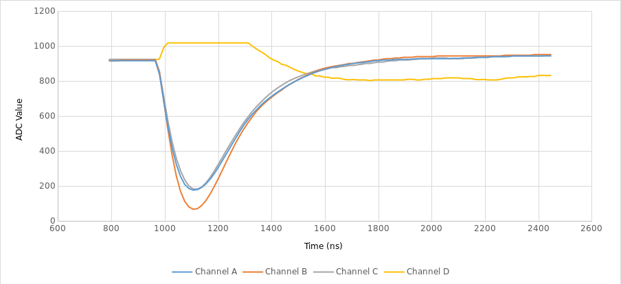
It was also noticed during experimentation with the ADC board that with a bias voltage of -31.5V the output from the amplifier board was regularly clipping. In order to improve the range of values obtained the bias voltage was reduced to -28.5V which has makes clipping much rarer.
ADC Board Software and Testing
The original FPGA code used to test the ADC recorded samples from the ADC into internal RAM which could be read out after the event over SPI. It contained logic to trigger once certain conditions were met (initially based on the sum value of all channels being below a threshold for a certain amount of time, similar to the original pre-ADC code); and also wrote to memory continuously with a pointer that wrapped around meaning samples before the start of the event were also captured.
The FPGA code was updated in order to minimise the requirements on the microcontroller; increasing the frequency of events that can be logged. Instead of recording all the samples; it only records the minimum value reached on each channel which should be related the number of coincident photons. In the future some other values (such as event length) may also be measured.
A small board using an STM32 microcontroller was also built that fitted on top of the new ADC board replacing the power supply board and seperate data logging board for a more compact system. This has space for its own microSD card and LoRa radio; or could connect over I²C/serial to another microcontroller. It also features USB for use with a PC during testing. In addition, to provide instant feedback during ground testing a speaker was added which beeps every time an event occurs; the frequency of the beep proportional to the energy of the event.
Hopefully this new setup will be flown on a future HAB flight, in which case an update with the obtained data and an evaluation of its perfomance will be posted. Unfortunately the relatively high build cost and fairly complex construction means we have not wanted to fly the SiPM experiment on a HAB flight where there is a reduced chance of recovery.
I am also investigating the possibility of using lower-cost, lower resolution ADCs but having a complete set of 16 ADCs covering all channels - this would give more potential for determining the direction of incident particles.
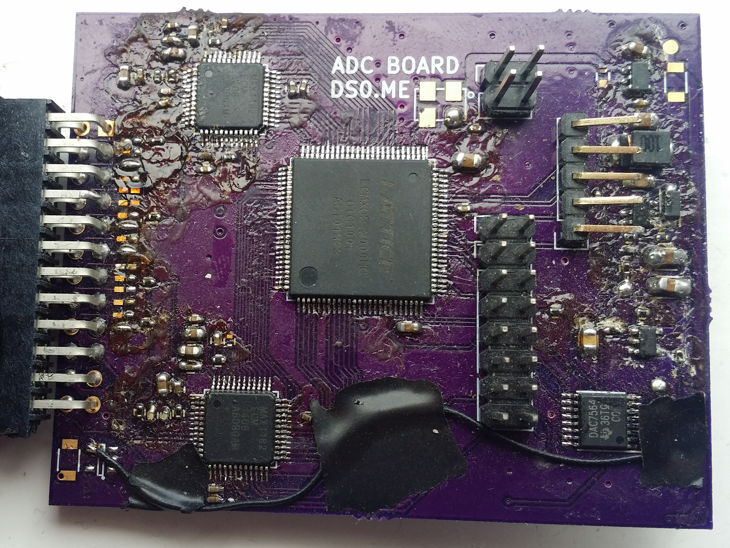 ADC Board
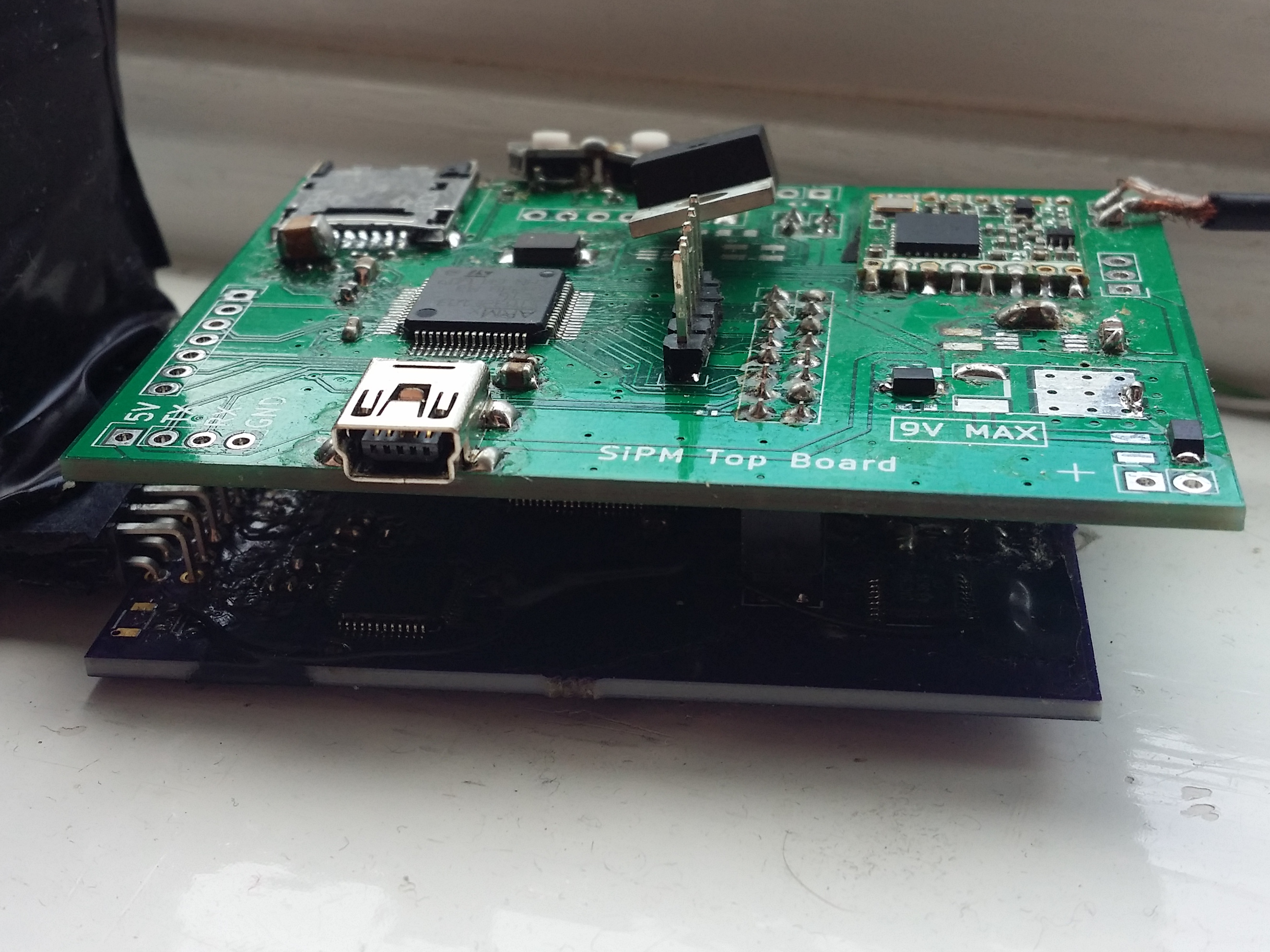 STM32 Board stacked on ADC Board
Project Repositories
- Biscay_Blueeye: original hardware and software
- SiPMADC: ADC board design
- SiPMMCU: new STM32 datalogging board