 Top Board (Digital)
These are smaller electronic projects which I have built over the years, and I don't deem worthy of a full article.
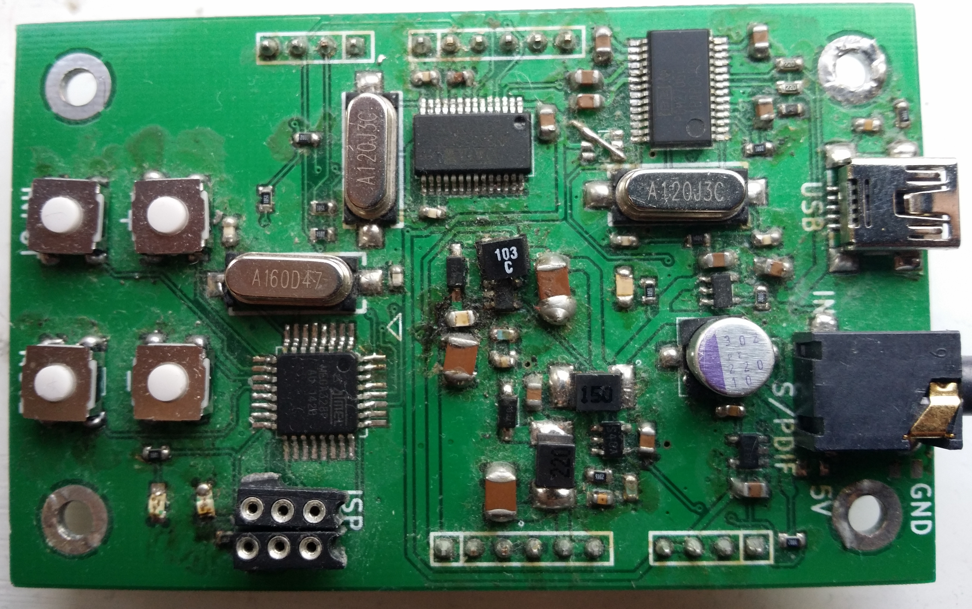
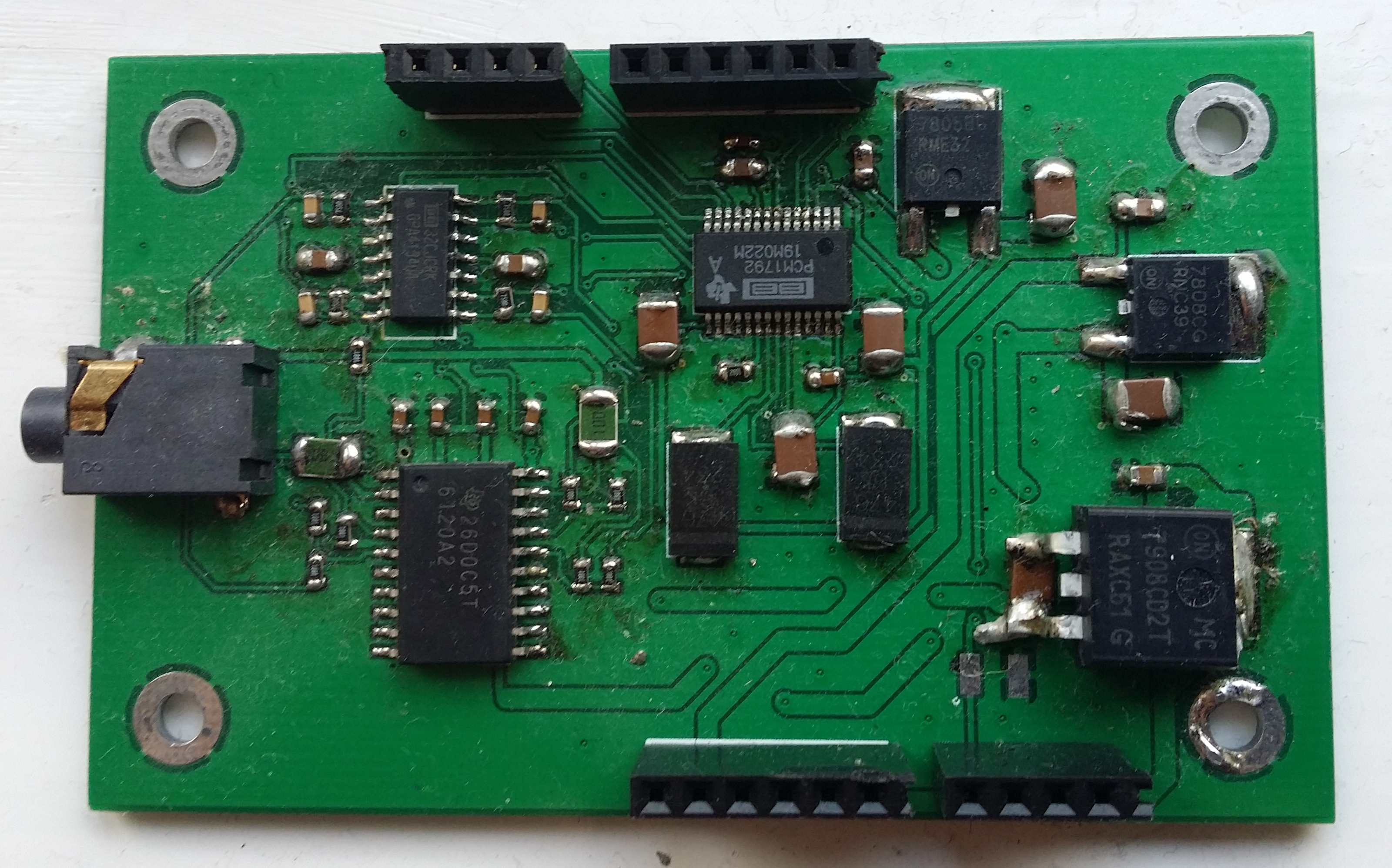
This was a project to make a high performance USB audio DAC and headphone amplifier without resorting to full "audiophoolery". It is designed as a two board system. The first board processes the digital audio and contains switching regulators to generate a bipolar ±10V supply from the USB 5V. The second board is the analogue board; containing the DAC itself and the headphone amplifier as well as linear regulators reducing the analogue supply to ±8V to minimise noise.
The USB interface is handled using TI PCM2705, which provides an S/PDIF output (the analogue output from this chip is not used as it's performance was deemed too poor, particularly in terms of SNR). The S/PDIF signal is converted to I²S for the DAC using a Cirrus Logic WM8805. An auxilliary S/PDIF input is also provided; allowing use with an S/PDIF source and at bit depths/sample rates higher than 16/48kHz. As well as the voltage regulators, the digital board also has an ATmega328P microcontroller for system control purposes. Its main task is to monitor the volume and input buttons; and update the DAC/WM8805 settings as needed over I²C. The audio board uses a PCM1792A DAC; OPA4134 op amp for I/V conversion; and TPA6120A2 amplifier as the final headphone amplifier.
The end result has performed very well for a few years. I have never noticed any background noise, unlike many integrated and cheaper sound cards. It has been used with both low-impedance and high-impedance headphones; and has even been used to drive 8Ω speakers at a low but acceptable volume.
Top Board (Digital)
 Bottom Board (DAC+Analogue)
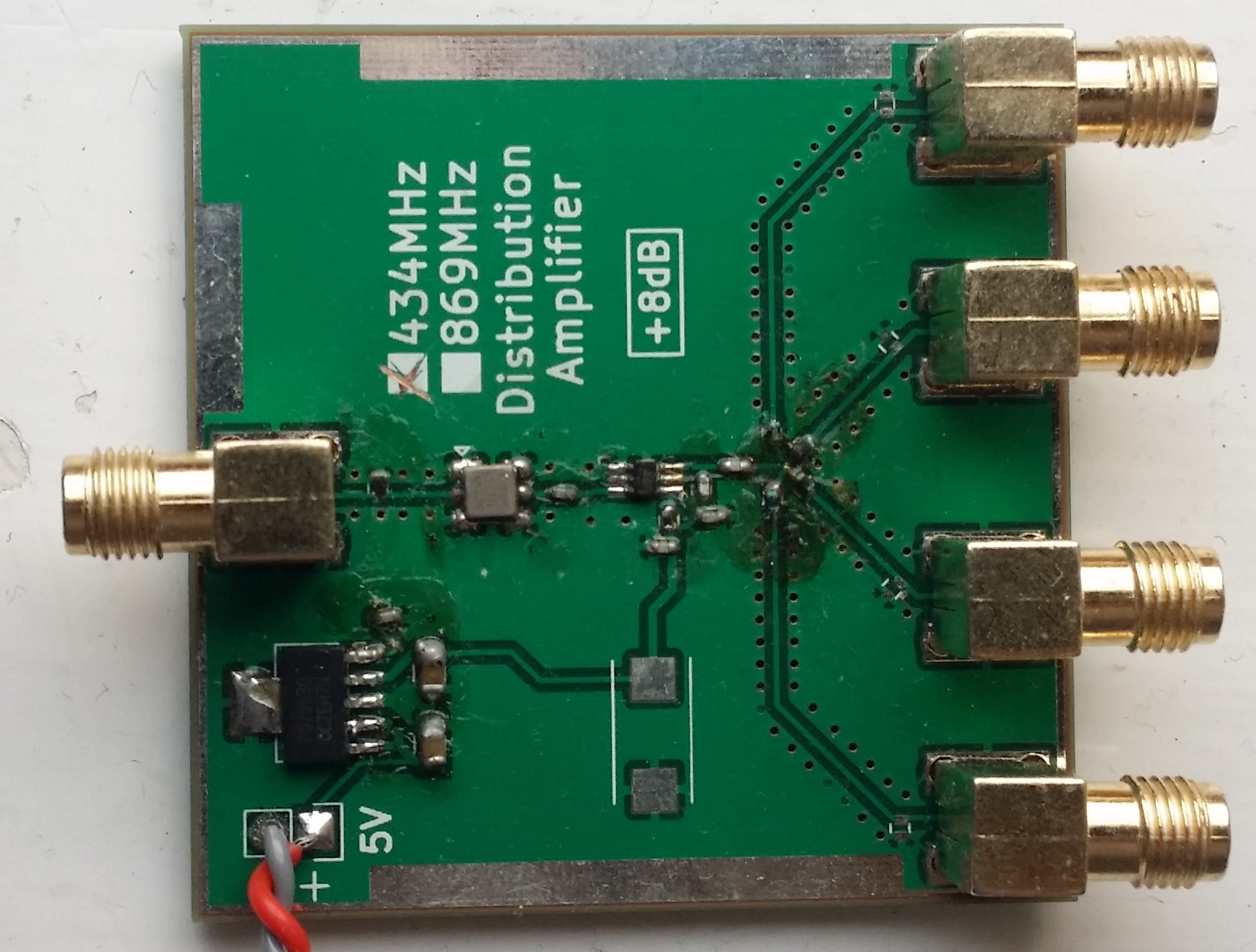
This was intended primarily for a high altitude balloon project where we were likely to need to track multiple balloons and also ideally wanted backup receivers in case a computer crashed. We were using LoRa radios at both 434MHz and 869MHz, so I designed the board so it could be built for both frequencies. It consists of a TDK SAW filter (B3710 or B3725) for improved out-of-band noise rejection, particularly useful in the 869MHz band; a Macom MAAL-010704 LNA and an inductive splitter going to the 4 output SMA connectors. There is also an onboard 3V LDO allowing it to be powered from a 5V supply.
Unfortunately I don't have the equipment to test a device like this properly, however a quick test using background noise and an RTLSDR dongle suggested it was working well. Actual performance in use has also been very good.
 434MHz Distribution Amp
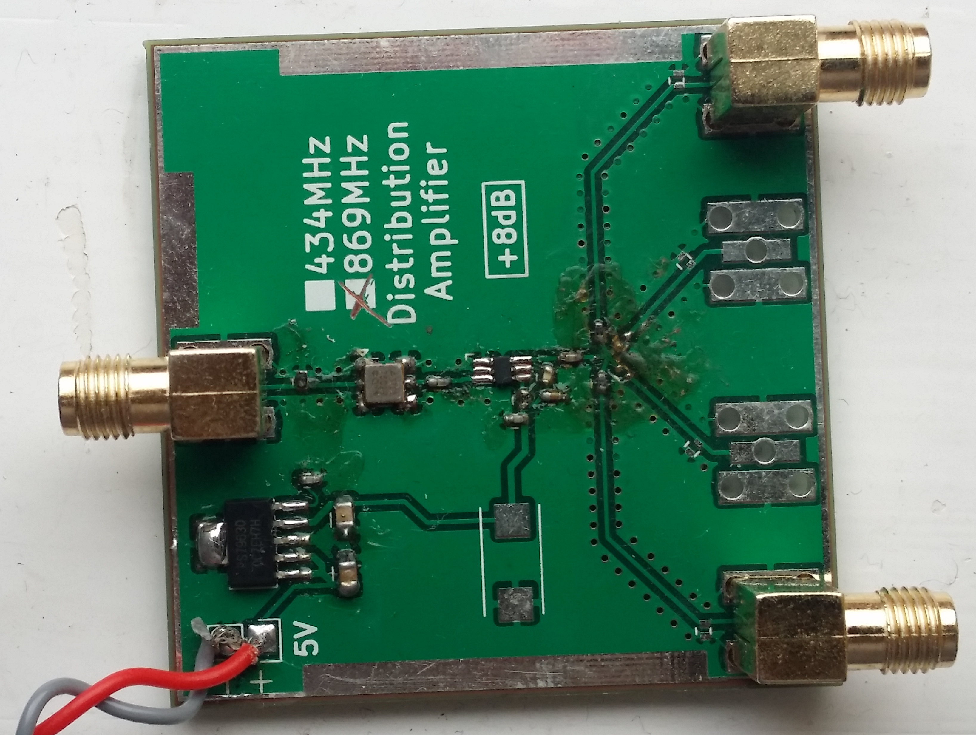 869MHz Distribution Amp
Design Files (KiCad + Gerbers) on GitHub
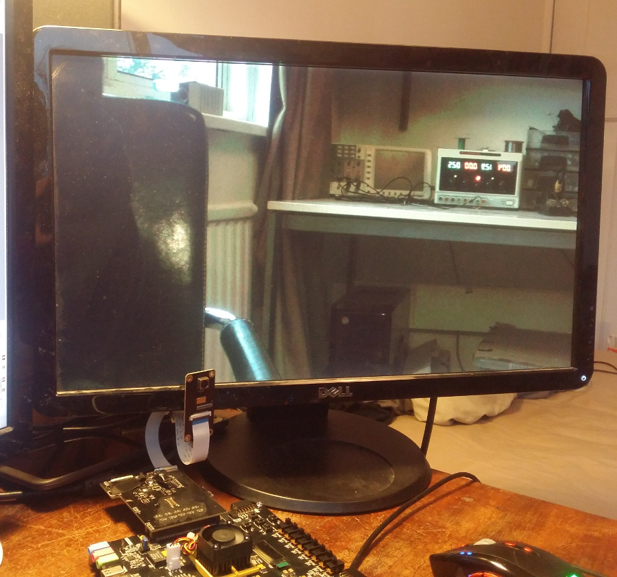
In order to develop test my open source MIPI CSI-2 and MIPI DSI IP cores, I needed some suitably advanced hardware to test them on. In the end I decided to use Firefly RK3288 camera boards, which themselves use an Omnivision OV13850 camera module capable of 4k at 30fps, which connect to the FMC board via flex cables. The board has two camera connectors for stereo video development. It also has a connector for a Sony Xperia Z5 Premium 4k LCD, although this interface is still in development. A resistor network is used to level shift the FPGA's output signals to D-PHY signalling levels, which is suspected to introduce SI issues at very high speeds. The camera interface performs very well however, reaching at least 4k at 48fps and 10bpp (line rate of 1.45Gbps/lane, 5.80Gbps total).
The designs are open source and published on GitHub.
 Testing the first revision of the FMC board
Due to having access to a number of 3.5" 320x240 LCDs (LQ035NC111) ideal for FPGA projects, I decided to design a board that would allow these to be connected to an FPGA dev board using a dual PMOD interface. In order to allow high colour depths with minimal pins, the LCD can be used in serial RGB or YUV422 modes. The board also contains a boost converter for the backlight LEDs.
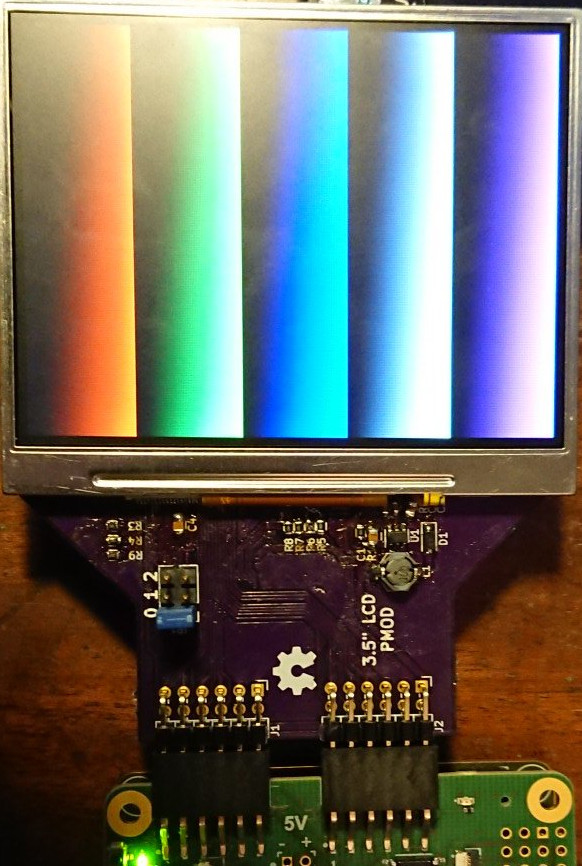 LCD PMOD connected to an icoBoard
The PCB designs are located on GitHub, along with a simple reference design. You can also purchase bare PCBs from the OSH Park shared project (this also has some assembly notes).